This article analyzes the architecture and detailed operation of negative buck topology. It will also discuss the circuit implementation of the topology from a system perspective to the building of the required circuit blocks, and include examples on building a voltage converter circuit, which is the key block for implementing a negative buck regulator using readily available boost ICs.
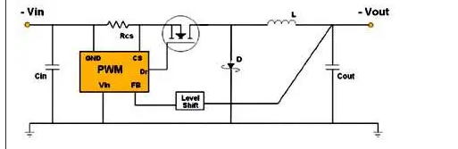
Figure 1: Basic architecture of a negative buck topology
Negative buck topology
Figure 1 shows the basic architecture of a negative output buck converter. Similar to a positive output buck converter, it has a high-side load switch, an LC filter, and freewheeling diode between the input and output. The difference between the two is the gate drive required to control the IC and feedback circuit.
In a positive buck, a typical negative-channel FET (NFET) used as a high-side transmission device requires a higher (more positive) gate drive voltage than the system’s input voltage (Vin) to switch on. Since the input voltage is already positive in the system, a special circuit is needed to generate higher voltages.
This feature is usually built into positive buck ICs. In a negative buck, a negative-channel FET (NFET) used as a high-side transmission device requires a more positive gate drive voltage than the system’s input voltage (Vin). In this case, a special circuit is not required since this input voltage is negative in the system.
All other voltages, including the output, are “higher” (more positive) and the converter ground is the positive voltage in the system. Under these circumstances, the converter can be implemented using a low-side FET pulse-width modulator control IC such as a boost/flyback regulator or controller.
A variety of ICs are available to implement negative output buck converters, including controllers and integrated monolithic switching regulators with low-side NFETs. Monolithic ICs are simple, easy to implement with fewer components. Controllers provide greater flexibility when higher output currents are required and efficiency and heat dissipation need to be optimized.
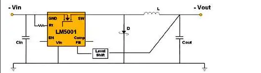
Figure 2: This negative buck topology uses a monolithic LM5001 boost/flyback regulator
Figure 2 shows a simplified diagram of a 3.1-75V input voltage boost/flyback regulator with a negative buck topology and a built-in 75V, 1A NFET.
In conventional boost applications, a gate drive voltage of a few volts above ground is supplied to its built-in N-channel MOSFET to turn it on. In negative output buck applications, the gate driver will still output a gate voltage a few volts higher than the IC ground pin, which is related to the input voltage (-Vin) of the system and will produce the needed results.
Unlike a conventional boost, but similar to a conventional buck, the peak IC switch current in Figure 2 is the same as the peak inductor/output current, thus allowing a 1A boost IC to be used for output currents up to 1A. Other regulators with different ratings would be used for higher or lower switch currents. A controller similar to the configuration shown in the figure can be used.
Voltage Converters
Another special consideration in negative output buck architectures using off-the-shelf boost ICs is the signal conditioning required for the feedback path. The feedback (FB) pin of most ICs requires a voltage of about 1.25V (relative to their ground) to maintain regulation. This voltage is usually obtained from the output (Vout) and is simply scaled down through a voltage divider network.
This technique easily allows the applied voltage to rise and fall as the output drops, which is necessary to maintain proper regulation. When this approach is used in a positive output buck, the FB voltage and output voltage are naturally referenced to the system ground and IC ground pins, thus regulation and conversion are not required.
In a negative output buck application using a low-side FET boost IC, the output (-Vout) and any of its divided voltage samples are still referenced to the system ground. However, since the IC ground pin is connected to -Vin instead of the system ground, the IC will not be able to read the FB voltage correctly (nor will it maintain regulation correctly), thus this voltage will need to be converted so that it is referenced to the IC ground pin.
This voltage conversion is indicated by the small box labeled “Level Shift” in Figures 1 and 2. There are multiple ways to implement this in hardware.
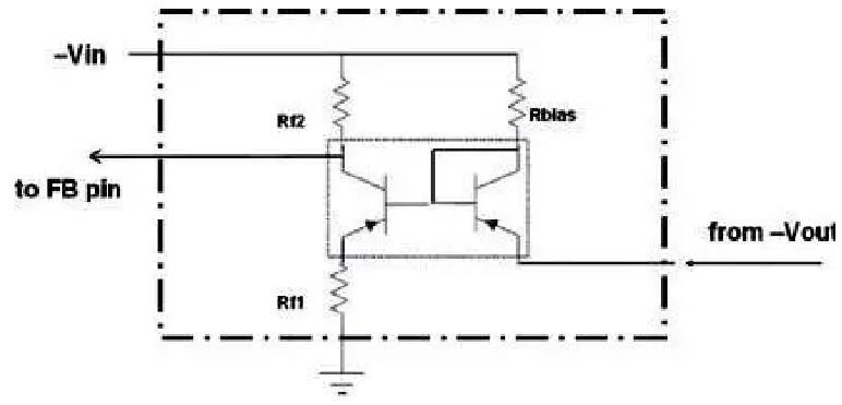
Figure 3: Voltage conversion can be implemented in hardware using a current mirror built with two PNP transistors.
Figure 3 shows a simple, common and possibly cheaper method of voltage conversion. It uses a current mirror built with a few inexpensive PNP transistors. Matching is recommended for performance and regulation accuracy.
Matched pairs can be found in single packages, with the DMMT3906 as a good example. In Figure 3, Rf1 and Rf2 narrow down the mirror voltage and are used to set the output voltage of the regulator (just like any adjustable regulator). In other words, the feedback gain for |Vref /Vout| and |Vout| is Vref x Rf1 / Rf2, where Vref is the IC feedback pin (reference) voltage. A variation of the current mirror circuit is shown below in Figure 4.
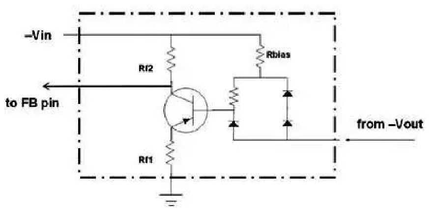
In this circuit, a single PNP transistor is used. D1 provides output voltage temperature compensation by eliminating the temperature drift effect of Q1’s PNP emitter-base voltage. D2 and D3 provide some pre-regulation for the bias current required by D1, thereby improving line regulation and ripple rejection by twofold.
Performance can be further improved by replacing the two series-connected diodes with a voltage reference, such as the LM385-1.2 or LM4040-2.5.
To simplify the circuit, or if the input voltage is relatively constant and the ripple is small, D2 and D3 can be eliminated and the bias resistors combined. Furthermore, eliminating D1 will result in a negative temperature coefficient on the output voltage.
Operational Amplifier
Designers who prefer the advantages and simplicity of operational amplifiers compared to discrete components can use operational amplifiers to implement voltage converter circuits.
Designers who prefer the advantages and simplicity of over-designing operational amplifiers with discrete components can use operational amplifiers to implement voltage converter circuits.
By connecting the operational amplifier in a configuration similar to the one used when sensing and amplifying differential voltages, it can be used in a negative output buck configuration to scale down the output voltage proportionally. This makes it suitable for the FB pin (thus setting the regulator’s output voltage) while shifting the reference for this voltage from the system ground to the -Vin rail.
The specific operational amplifier used depends on the application requirements, but a general-purpose operational amplifier will suffice. A low input offset voltage is important for the regulator’s voltage accuracy, and the operational amplifier needs to have a common-mode voltage range greater than the Vout amplitude.
Conclusion
A variety of boost/flyback regulators are available to implement negative output buck converters. Voltage regulators and controllers with wide input voltage ranges are used as examples due to their flexibility in a wide range of applications.
Similar to a buck converter, the switch current is the converter’s output current and the inductor value should also be selected using the ripple current. Like a conventional positive buck converter, this topology does not have a right half-plane zero.
If a voltage conversion circuit is used, such as the one in Figures 3 or 4, it is evident that compensation can be flexible as adding poles or zeros is as easy as adding a capacitor in parallel with Rf1 (zero) or Rf2 (pole).